About
This is a tutorial for panelizing (producing a panel comprising replicates of a small PCB) in KiCad.
The goal is a separate design, a panel comprising a horizontal row of my boards separated by the 100 mil routing width that my fab uses. The purpose is a panel that is an easily handled batch during assembly (solder paste stenciling, placing SMD components, and moving to the reflow oven.)
This is specialized:
- uses KiCad
- replicates one small board,
- I don’t design internal support tabs
- I don’t design a frame around the replicates
- it’s a manual operation using fiducials and block copying
In this example, I assume the fab is OHSPark:
- requires 100 mil separation
- they will add internal and external support tabs
- they don’t require a frame (since I will accept if the panels break apart in shipping.)
Internal support tabs hold the panel together. External support tabs hold my panel in the larger panel that the fab makes.
There might be other ways to do this. At one time there existed Python scripts to automate this.
Overview of the process
Use fiducials (layer alignment targets.) Create an initial fiducial pair at grid size 100 mils. Use a minimum grid size( 0.01mm) and nudging with the arrow keys when aligning copies. Use block copy to copy both the PCB and nearby fiducials.
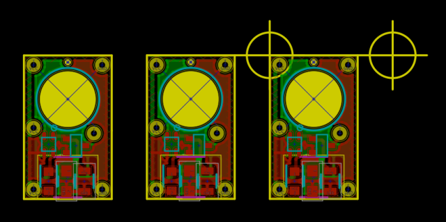
Here is a picture of the nearly finished result:
Before you start
You have a finished existing board design. (Any changes to it will not automatically flow into your panel design. You will need to redo your panel if the child PCB changes.)
Your zone outlines and all other components are within your PCB edge outline ( simplifies block copy.)
The line width of your board outline (in Edge.Cuts layer) is small (say the default of 0.15 mm). This matches the line width of fiducials, making it easier to see when your board outline is corner aligned to a fiducial. (Your fab cuts to the center of the graphic line defining the edge.)
Your existing board design need not be aligned to any particular grid size. Your board size need not be a multiple of any particular grid size. (Although it might be easier if your board is aligned to a 100 mil grid and a multiple of 100 mils in size.)
The process
Starting PCBNew app
Click on the PCBNew icon (in your desktop, launcher, or file browser.) Expect a window showing an empty PCB design. (Note you can’t start PCBNew from within your existing project, since then it opens your existing design, that you should keep separate.)
Import your existing PCB into the empty panel design
Choose File>Append Board. Expect a file browser to open.
Select the foo.kicad_pcb file of your existing PCB design and choose the OK button. Expect a floating view of your existing PCB design.
Click in the sheet anywhere to place the first copy of your PCB.
Add two fiducials on a 100 mil grid
Choose ‘100 mils’ from the grid combobox in the toolbar. Expect the grid to change.
Select the fiducial tool by clicking in the “Add layer alignment target” icon in the right toolbar. Expect the cursor to change to a pencil icon. Click in the sheet near the upper right corner of the PCB copy. Expect a fiducial symbol placed on the sheet, snapped to the nearest grid point. (It is in the Edge.Cuts layer.)
Repeat, placing another fiducial 100 mils to the right of the first fiducial.
Align the first replicate’s upper right corner to the left fiducial
Choose ‘0.01 mils’ from the grid combobox in the toolbar.
Zoom in so you can see precise alignment.
Choose the pointer tool.
Drag out a rect around the PCB. Expect a “Block Operation” dialog to open. Choose the OK button. Expect an image of the PCB to follow the cursor (an the original to remain visible.)
Align upper right of the first replicate to the fiducial’s cross, and click the LMB (left mouse button.) Expect the PCB to be placed.
Delete the left fiducial
Using the pointer tool, click the RMB (right mouse button) on the left fiducial. Expect a context menu to pop up. Choose “Delete Target.”
Block copy the PCB and fiducial
Using the pointer tool, drag out a rect around the first PCB replicate and the fiducial to its right. Expect a “Block Operation” dialog to open. Choose the OK button. Expect an image of the PCB and fiducial to follow the cursor, but for the original also to be visible.
Align upper left of the dragged copy to the fiducial of the original. Click the RMB ( right! mouse button.) Expect a context menu to pop up. Choose “Copy Block”. Expect a second replicate of your PCB to be placed.
(Also expect horizontal rat’s nest lines to appear, connecting nets in the left copy to nets in the right copy. You can ignore those, or “Hide board ratsnest”.)
Note that unless your board is a multiple of 100 mils wide, the newly copied fiducial won’t be on a 100 mils grid.
Repeat
Delete the left fiducial and again copy the right PCB ( or many of them) and the fiducial to its right.
You might make a few more copies. You should not make more copies than will fit in the larger panels used in the fab.
Delete fiducials
KiCad puts fiducials in the Edge.Cuts layer. Some fabs (OSHPark) might deal with this as you expect, while other fabs may route out (drill) the fiducials! A post on the KiCad forums discusses this.
You should probably delete the fiducials, so you don’t worry about how your fab interprets them.
Save As
Choose File>Save As and so forth to save the panel design. You probably should create a separate folder to put it in. In that separate folder, you can also put the Gerbers for the panel.
(If you choose File>Save you might get an error message, probably because on some platforms, KiCad attempts to save in the locked directory of the application file.)
Finishing up
You might want to run the DRC. It should still work.
You now can plot Gerbers and generate a drill file. (It seems like you must choose an absolute path for the drill file, else KiCad attempts to write it in a locked app directory?)
One advantage of a panel such as this: the solder mask Gerber layer will precisely align with the boards of the panel. (You don’t need to panelize a solder paste stencil like you might for a happenstance panelization that the fab might create and deliver to you.)
Accuracy
I don’t think you need to be super accurate. When I do it, the alignment seems a few pixels off, less than a mil off. Use the arrow keys while dragging to nudge your PCB a few pixels.
Even if the distance between your PCB copies is a few mils off, the fab actually uses a router bit that is smaller than 100 mils (it cuts on the way into a slot, moves over, and cuts on the way out.)
If the outer edges of your panel are a few mils off, your panel will still probably fit in the jig for your solder paste stencil.
In other words, don’t worry about a few mils, because your home hobbyist processes don’t require that accuracy.
Disclaimer
I haven’t tested this with OSHPark yet.
